Key Takeaways
- PCB manufacturing involves multiple precisely controlled steps, including material preparation, layer imaging, drilling, plating, and final inspection, to ensure functionality and reliability.
- Engineers use specialized CAD software for schematic capture, layout, and routing, creating accurate designs that optimize performance and manufacturability.
- Key fabrication processes like photolithography, lamination, drilling, and through-hole plating are essential for building complex multi-layer PCBs with high-density circuitry.
- Application of solder mask, silkscreen printing, and surface finishes such as HASL, ENIG, OSP, or immersion coatings protect circuits and ensure assembly readiness.
- Stringent quality control measures, including automated optical inspection (AOI), electrical testing, and X-ray analysis, guarantee PCB accuracy and compliance with international standards before shipment.
PCB manufacturing involves multiple precisely controlled steps including material preparation, photolithography, drilling, plating, and rigorous quality control to create reliable circuit boards for modern electronics. The process begins with substrate preparation and copper layer bonding, followed by photoresist application and UV exposure to define circuit patterns. Leading manufacturers like OurPCB utilise automated systems, stringent inspection protocols, and compliance with IPC-6012 standards to ensure consistent quality and reliability for diverse electronic applications.
Understanding the PCB Manufacturing Process
PCB manufacturing uses set steps to produce high-precision circuit boards needed for electronic assemblies. Companies like OurPCB in China apply automated systems to improve consistency and accuracy during production.
Fabricators start with substrate materials, usually FR4 fiberglass, which provide insulation and mechanical support. Copper layers bond to the substrate, then computer-controlled machines add photoresist, a light-sensitive coating, to define circuit patterns. Photolithography exposes these coated panels to UV light, transferring the circuit image before etching solutions remove unwanted copper.
Drilling forms holes used for electrical connections and mounting. CNC drilling systems at OurPCB create plated-through-holes and vias critical for multi-layer connectivity. Next, through-hole plating deposits copper inside holes, linking circuit layers for reliable current flow.
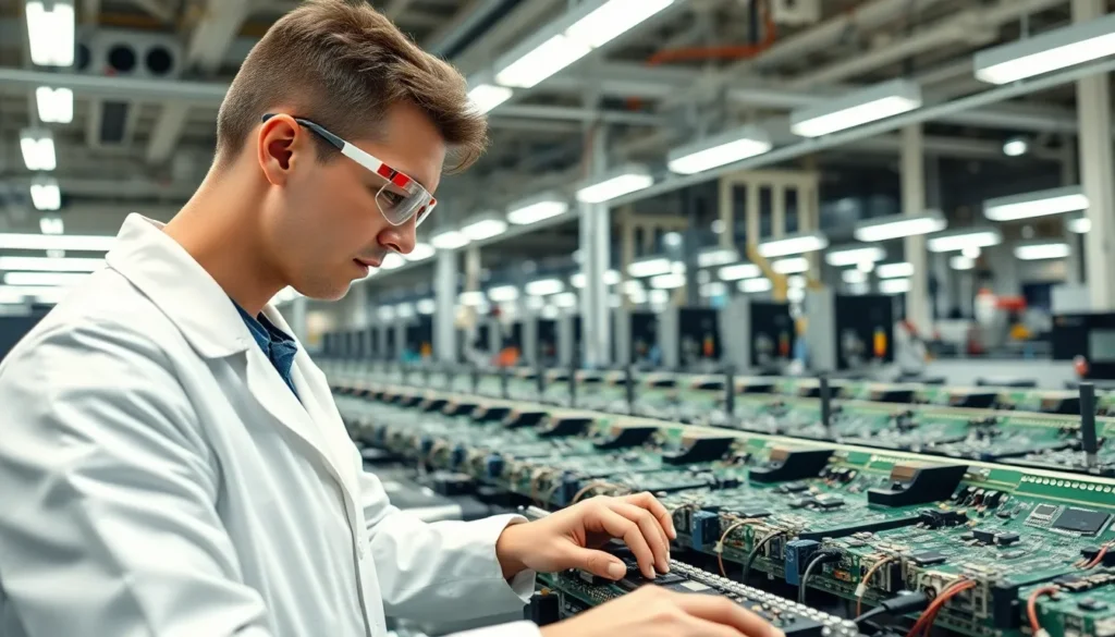
Solder mask application isolates conductive traces while exposing pads for soldering, then silkscreen printing adds reference designators and component labels. Automated optical inspection (AOI) checks finished boards for defects, verifying alignment and trace integrity. OurPCB runs electrical tests, confirming every pathway conducts as designed.
Finalizing the production process, panels are routed into individual boards. OurPCB packages completed PCBs according to customer requirements for worldwide delivery, supporting high-volume orders and rapid prototyping.
Designing the PCB Layout
Engineers use PCB layout design to define the electrical and mechanical features of circuit boards. Precise layout and routing optimize performance, manufacturability, and reliability for high-volume assembly at facilities like OurPCB in China.
Schematic Capture
Schematic capture creates a digital diagram showing component connections for a PCB. Designers use CAD software like Altium Designer or KiCAD for drawing, symbol assignment, and netlist generation. OurPCB supports files from these platforms, ensuring smooth data transfer. Each symbol represents components such as resistors and microcontrollers, while lines indicate electrical pathways. Accurate schematics reduce errors during prototyping and mass production.
Layout and Routing
Layout and routing arrange components and define copper traces on the PCB. Designers place parts on the board, balancing electrical needs and manufacturability. Automated routing software minimizes trace length and avoids crosstalk for dense circuitry. OurPCB checks submitted Gerber files for compliance with equipment tolerances and DFM (Design for Manufacturability) guidelines. Layer stack-ups and clearances align with client and IPC standards to optimize electrical performance and yield during fabrication.
Preparing the Materials
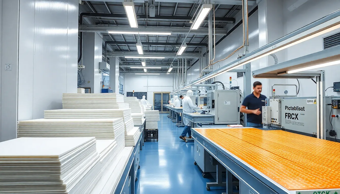
PCB manufacturing starts with selecting substrate materials. Common substrates include FR4 fiberglass, aluminum, or polyimide, each supporting different performance requirements. OurPCB sources FR4 for multilayer PCBs used in computers and industrial equipment.
Copper foils are bonded to the substrate to form conductive layers. Typical copper thickness ranges from 18µm to 70µm, depending on current requirements and PCB design. Factories like OurPCB maintain copper purity and sheet cleanliness to avoid trace defects.
Dry films called photoresists are applied to the copper for subsequent photolithography steps. The selection of negative or positive photoresist depends on trace patterning methods. Environmental controls at OurPCB reduce contamination before etching and plating.
Pre-cut panels are prepared to match final PCB dimensions and panelization needs. Standard panel sizes include 18″x24″ and 21″x24“, optimizing throughput in automated lines. OurPCB adjusts panel sizes for customer-specific projects.
Material traceability is maintained from receipt to assembly. Digitized batch codes, certifications, and inspection reports are attached to each lot at OurPCB, supporting IPC-6012 and ISO 9001 standards.
Fabricating the PCB Layers
Fabricating the PCB layers creates the conductive and insulating structures that define circuit function. OurPCB applies strict controls over each step to maintain electrical reliability and meet IPC-6012 standards.
Inner Layer Imaging
Inner layer imaging defines the copper circuitry that forms internal connections in multilayer PCBs. OurPCB laminates copper foil onto FR4 cores, coats panels with light-sensitive photoresist, and exposes circuit patterns using UV light and precision photomasks. Automated development lines remove unexposed photoresist, leaving protected copper features. Dimension accuracy, maintained within ±25µm, ensures consistent trace separation for high-speed and high-density boards. OurPCB uses inline AOI inspection to verify trace widths and detect shorts or opens before further processing.
Etching and Cleaning
Etching and cleaning remove unwanted copper from inner layers, finalizing signal and ground patterns. Automated etching tanks dissolve exposed copper after imaging, using controlled chemical concentrations to avoid undercutting traces. Copper thickness targets, like 35µm for standard layers, are verified with XRF meters. Rinsing systems eliminate residual chemicals and debris. OurPCB inspects etched panels for uniformity, ensuring defect-free surfaces. Final cleaning removes organic contaminants, preparing inner layers for lamination into multilayer stacks.
Layer Alignment and Lamination
Layer alignment and lamination ensure multilayer PCB integrity at OurPCB. Automated optical alignment systems register each inner etched layer using high-contrast fiducial marks, holding positional tolerance within ±20µm. Precision pin-lamination presses then stack inner copper layers, prepreg insulation sheets, and external copper foils. High-pressure (up to 25 MPa) and elevated temperature (up to 200°C) cycles activate resin flow in the prepreg, bonding all layers into a rigid unit while eliminating air gaps and voids.
OurPCB uses vacuum-laminating chambers to improve resin penetration and achieve even dielectric thickness across the PCB surface. This process prevents delamination and ensures high-voltage reliability in client applications like server motherboards and automotive controllers. Each laminated panel receives automated edge trimming within ±0.1 mm tolerance, supporting consistent layer reveal and enabling subsequent drilling. Workers verify stack height and layer registration on every lot, in line with IPC-6012 qualification criteria. Digital batch records at OurPCB link each laminated batch to its corresponding inspection data, substrate lot, and engineering revision for traceability and quality control.
Drilling and Plating Through Holes
Drilling and plating through holes create reliable electrical connections between PCB layers. CNC drilling machines at OurPCB bore holes ranging from 0.15mm to 0.8mm diameter, matching design specifications for components like vias, headers, and press-fit pins. Laser drilling supports microvias in HDI and flexible PCBs for higher interconnect density.
Automated cleaning removes debris from drilled holes, preventing plating defects. Direct metallization lines deposit a thin seed layer, usually 1–2µm of electroless copper, on the wall of each hole. This layer forms the foundation for copper electroplating, which builds up to 20–25µm thickness for robust interlayer conductivity.
Process monitoring at OurPCB verifies plating thickness using X-ray fluorescence (XRF). AOI inspection checks for voids or partial coverage. Cleanroom controls maintain process quality, especially for high-reliability boards used in telecom and industrial control.
Drilled and plated-through-hole quality at OurPCB meets IPC-6012 standards. Plating distribution, aspect ratio, and adhesion are backed by batch-level inspection records, supporting traceability for every production lot.
Solder Mask and Silkscreen Application
Solder mask covers PCB surfaces to protect copper traces and prevent solder bridging during assembly. OurPCB applies liquid photoimageable (LPI) solder mask using automated coating lines for uniform 15µm–30µm film thickness, supporting reliability in high-density server, medical, and automotive PCBs. Green solder mask dominates global orders, though colors like black, blue, white, and red are available. Precision exposure and development create openings for pads and vias, matching IPC-SM-840 standards.
Silkscreen printing adds component outlines, polarity indicators, and reference designators to the PCB surface. OurPCB uses non-conductive epoxy inks and automated inkjet systems for accuracy, ensuring clear identification on 0.20mm text or barcodes. These markings support assembly, inspection, and traceability, especially when complex boards for telecom or industrial controls require rapid verification. Silkscreen layer contents follow client CAD files and are verified against assembly documentation before production proceeds.
Surface Finishing Techniques
Surface finishing techniques preserve solderability and protect exposed copper features on printed circuit boards. Surface finish selection depends on application, assembly process, component type, and end-user reliability requirements.
- HASL (Hot Air Solder Leveling): HASL, commonly used at OurPCB for industrial and consumer electronics, coats copper traces with molten solder then removes excess via hot air knives. This method enables robust mechanical protection but introduces minor surface unevenness that may affect ultra-fine pitch components.
- ENIG (Electroless Nickel Immersion Gold): ENIG, often specified for high-density interconnect boards and BGA footprints, forms a uniform, planar surface by depositing a thin nickel barrier and a gold top layer. OurPCB ensures thicknesses of 3–6 µm for nickel and 0.05–0.1 µm for gold. ENIG resists corrosion and supports gold wire bonding.
- OSP (Organic Solderability Preservative): OSP, applied to low-cost high-volume PCBs at OurPCB, is a water-based organic coating that shields copper from oxidation before soldering. OSP is suitable for automated SMT assembly lines but does not withstand multiple solder reflow cycles.
- Immersion Silver and Immersion Tin: Immersion silver and tin finishes provide planarity for high-frequency and fine-pitch devices, as seen in telecom or server motherboards. OurPCB applies immersion silver at 0.1–0.3 µm and immersion tin at 0.8–1.2 µm thickness, balancing cost with performance stability.
Surface finishing quality is verified at OurPCB with X-ray fluorescence (XRF) measurement and adhesion testing, supporting IPC-6012 and RoHS compliance for global electronics production.
Final Inspection and Quality Control
Final inspection and quality control at OurPCB confirm that each PCB meets customer specifications and international standards before shipment. Technicians perform automated optical inspection (AOI) on every panel to detect open circuits, shorts, and solder mask misalignment. X-ray machines check multi-layer registration and verify hidden solder joints for BGA and fine-pitch components.
Electrical testing validates circuit continuity and isolation, using flying probe or fixture testers depending on production volume and complexity. Testing covers 100% of boards for functionality according to IPC-6012 Class 2 or Class 3 requirements.
Dimensional inspection confirms panel size, hole diameters, solder mask clearance, and silkscreen accuracy meet tolerances defined in Gerber files. Surface finish integrity is verified via X-ray fluorescence (XRF) to measure thickness and composition of coatings such as ENIG, HASL, and OSP.
Technicians review traceability documentation, production logs, and previous defect data to prevent recurrence of process deviations. Final packaging takes place in anti-static environments with barcode labeling, moisture barriers, and ESD-compliant materials for safe global shipping.
About OurPCB
OurPCB is a leading provider of PCB manufacturing and assembly services, offering solutions such as turnkey PCB assembly, PCB design services, and rapid prototyping to bring your PCB concepts to life. Their comprehensive services cover everything from initial design consultation to final product delivery, ensuring high-quality printed circuit boards for various electronic applications. Whether it’s a simple prototype or a complex multi-layer PCB assembly, they are equipped to deliver reliable solutions for diverse electronic projects.
Contact:
Hommer Zhao, Owner
Phone: +1 626 790 1487
Email: [email protected]
Website: ourpcb.com
Location:
160 W Sierra Madre Blvd, Sierra Madre, CA 91024, USA
Frequently Asked Questions
What is a printed circuit board (PCB) and why is it important?
A printed circuit board (PCB) is a flat board that connects and supports electronic components using conductive tracks made of copper. PCBs are essential because they power nearly all modern electronic devices, from computers to industrial equipment, by providing reliable electrical connections and mechanical support.
What materials are commonly used to make PCBs?
PCBs are typically made using substrate materials like FR4 fiberglass, aluminum, or polyimide. FR4 is most commonly used, especially for multilayer boards in computers and industrial applications, due to its strength, stability, and good electrical properties.
How does the PCB manufacturing process begin?
The process begins with designing a schematic using CAD software to map out electronic connections. Then, materials like FR4 panels are prepared and copper layers are bonded. Next, photoresist is applied, and photolithography defines the circuit pattern before etching removes unwanted copper.
What is the role of photolithography in PCB manufacturing?
Photolithography is used to transfer circuit designs onto the copper clad board. A photoresist layer is applied, and UV light exposes the desired pattern, which is then developed and etched. This process precisely defines conductive copper paths on the board.
How does OurPCB ensure PCB quality and reliability?
OurPCB follows strict IPC-6012 and ISO 9001 standards, uses automated optical inspection (AOI), X-ray checks, and electrical testing. They track and document each batch for traceability, helping ensure that every board meets rigorous quality, safety, and reliability requirements.
Why is copper purity important in PCBs?
High copper purity is crucial for creating defect-free conductive traces, as impurities can cause signal loss, open circuits, or shorts, reducing reliability and performance in electronic devices.
What is Design for Manufacturability (DFM) in PCB design?
DFM ensures that PCB layouts are optimized for reliable, efficient mass production. This includes following design guidelines for layer thickness, hole size, spacing, and tolerances, which helps avoid mistakes during assembly and improves manufacturing yield.
What are the main steps in inspecting finished PCBs?
Finished PCBs undergo automated optical inspection (AOI), electrical testing, X-ray testing for multilayer alignment and hidden joints, dimensional checks against CAD files, and surface finish verification using XRF to ensure compliance with all specifications.
What are the common surface finishes used on PCBs?
Common surface finishes include HASL (Hot Air Solder Leveling), ENIG (Electroless Nickel Immersion Gold), OSP (Organic Solderability Preservative), immersion silver, and immersion tin. Each finish serves different needs for solderability and protection against oxidation.
Why is solder mask applied to PCBs?
A solder mask layer is applied over the copper traces to prevent solder bridging during assembly, which helps protect circuits from accidental shorts and environmental contamination, improving longevity and reliability.